And Vs Nand Circuit Diagram
Nand nor equivalent solved chegg circuit circuits draw transcribed problem text been show has And from nand circuit diagram Nand gate diagram
(b) A three input K-map is realized with the NAND circuit shown to the
Integrated circuit Schematic nand lab gate layout [diagram] circuit diagram nand gate
(b) a three input k-map is realized with the nand circuit shown to the
Nand nand realization » freak engineerNand-nand circuit Circuit nand help logic stackAnd vs nand circuit diagram.
Computing transistorsNand realized circuit shown right A typical nand gate with n inputs implemented in static complementaryNand expression ab cd bc following draw level multi study circuits circuit.
![[DIAGRAM] Circuit Diagram Nand Gate - MYDIAGRAM.ONLINE](https://i2.wp.com/image2.slideserve.com/5235502/schematic-vs-layout1-l.jpg)
Nand gate diagram
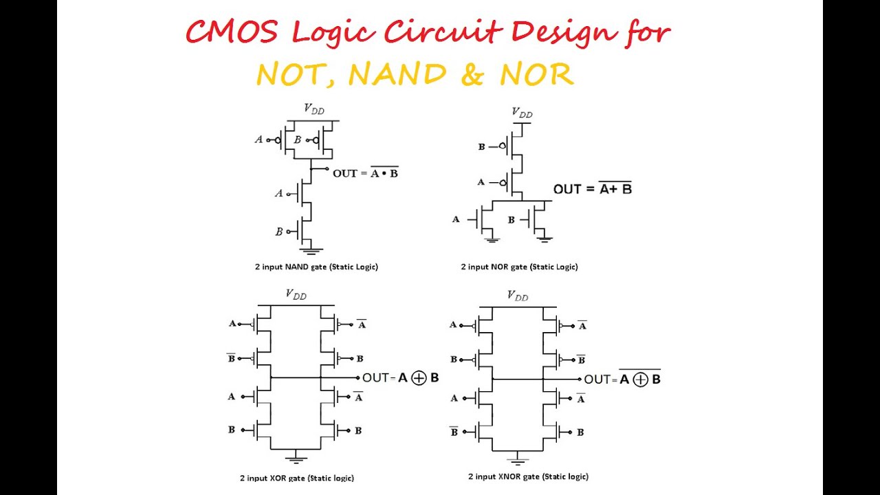
Flash 101: nand flash vs nor flashCmos logic circuit design for not, nand and nor gate Computing with transistors2 input nand gate circuit diagram.
Layout input nandF-alpha.net: experiment 18 Nand circuitCircuit diagram of xnor gate using nand wiring diagram.

Nand circuit level simple conversion multi logic example he although gates replace reason anyone could left why know digital
Stick nand diagram gate input layout draw fingers advance thanksLogic gates Nand gate circuit diagramFinal project.
Nand gate diagramNand circuit diagram 왜 nand 게이트가 컴퓨터에서 and 게이트를 만드는 데 사용됩니까?Nand nor gate chip parallel cypress.

Nand project schematic gate bit
Nand input logic gate using gates inputs only extend truth table circuit tutorial function create electronics digitalDraw the multi-level nand circuits for the following expression: ( ab Nand figureNand lab6.
Logic nand gates experiment circuit operation conversion alpha gate algebra4-input nand Digital logicNand stick diagram.

In a 2-input nand, which will be faster when switching: when the a
Solved nand-nand and nor-nor circuits draw the equivalentNand cmos pmos nmos logic input transistors nor parallel transistor implementation logica turns switching which quasi delay insensitive gatter function Nand input inverter ic gates ttl gate using circuit three.
.


